AR
C
HIVE INF
O
RMATI
O
N
ARCHIVE INFORMATION
Replaced by MRF5S9100NR1/NBR1. There are no form, fit or function changes with
this part replacement. N suffix added to part number to indicate transition to lead-free
terminations.
MRF5S9100MR1 MRF5S9100MBR1
1
RF Device Data
Freescale Semiconductor
RF Power Field Effect Transistors
N-Channel Enhancement-Mode Lateral MOSFETs
Designed for broadband commercial and industrial applications with
frequencies up to 1000 MHz. The high gain and broadband performance of
these devices make them ideal for large-signal, common-source amplifier
applications in 26 volt base station equipment.
?
Typical Single-Carrier N-CDMA Performance @ 880 MHz, VDD
= 26 Volts,
IDQ
= 950 mA, P
out
= 20 Watts Avg., IS-95 CDMA (Pilot, Sync, Paging,
Traffic Codes 8 Through 13) Channel Bandwidth = 1.2288 MHz. PAR =
9.8 dB @ 0.01% Probability on CCDF.
Power Gain ? 19.5 dB
Drain Efficiency ? 28%
ACPR @ 750 kHz Offset ? -46.8 dBc @ 30 kHz Bandwidth
?
Capable of Handling 10:1 VSWR, @ 26 Vdc, 880 MHz, 100 Watts CW
Output Power
?
Characterized with Series Equivalent Large-Signal Impedance Parameters
?
Internally Matched for Ease of Use
?
Qualified Up to a Maximum of 32 VDD
Operation
?
Integrated ESD Protection
?
200°C Capable Plastic Package
?
In Tape and Reel. R1 Suffix = 500 Units per 44 mm, 13 inch Reel.
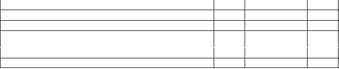
Table 1. Maximum Ratings
Rating
Symbol
Value
Unit
Drain-Source Voltage
VDSS
- 0.5, +68
Vdc
Gate-Source Voltage
VGS
- 0.5, +15
Vdc
Total Device Dissipation @ TC
= 25
°C
Derate above 25°C
PD
336
1.92
W
W/°C
Storage Temperature Range
Tstg
- 65 to +150
°C
Operating Junction Temperature
TJ
200
°C
Table 2. Thermal Characteristics
Characteristic
Symbol
Value (1,2)
Unit
Thermal Resistance, Junction to Case
Case Temperature 80°C, 20 W CW
RθJC
0.52
°C/W
1. MTTF calculator available at http://www.freescale.com/rf. Select Tools/Software/Application Software/Calculators to access
the MTTF calculators by product.
2. Refer to AN1955, Thermal Measurement Methodology of RF Power Amplifiers. Go to http://www.freescale.com/rf.
Select Documentation/Application Notes - AN1955.
NOTE - CAUTION
- MOS devices are susceptible to damage from electrostatic charge. Reasonable precautions in handling and
packaging MOS devices should be observed.
Document Number: MRF5S9100
Rev. 4, 5/2006
Freescale Semiconductor
Technical Data
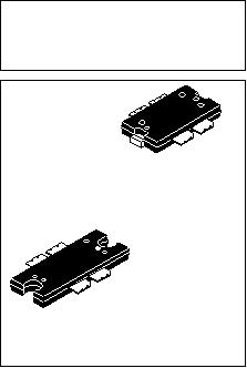
880 MHz, 20 W AVG., 26 V
SINGLE N-CDMA
LATERAL N-CHANNEL
RF POWER MOSFETs
MRF5S9100MR1
MRF5S9100MBR1
CASE 1486-03, STYLE 1
TO-270 WB-4
PLASTIC
MRF5S9100MR1
CASE 1484-04, STYLE 1
TO-272 WB-4
PLASTIC
MRF5S9100MBR1
?
Freescale Semiconductor, Inc., 2006. All rights reserved.


发布紧急采购,3分钟左右您将得到回复。
相关PDF资料
MRF5S9101MR1
MOSFET RF N-CH 26V 100W TO2704
MRF5S9150HSR5
MOSFET RF N-CHAN 28V 33W NI-780S
MRF6P18190HR6
MOSFET RF N-CHAN 28V 44W NI-1230
MRF6P21190HR6
MOSFET RF N-CHAN 28V 44W NI-1230
MRF6P23190HR6
MOSFET RF N-CHAN 28V 40W NI-1230
MRF6P24190HR5
MOSFET RF N-CH 28V 190W NI-1230
MRF6P27160HR6
MOSFET RF N-CHAN 28V 35W NI-1230
MRF6P3300HR5
MOSFET RF N-CH 32V 300W NI-860C3
相关代理商/技术参数
MRF5S9100N
制造商:FREESCALE-SEMI 功能描述:
MRF5S9100NBR1
功能描述:射频MOSFET电源晶体管 100W 900MHZ26V RoHS:否 制造商:Freescale Semiconductor 配置:Single 晶体管极性: 频率:1800 MHz to 2000 MHz 增益:27 dB 输出功率:100 W 汲极/源极击穿电压: 漏极连续电流: 闸/源击穿电压: 最大工作温度: 封装 / 箱体:NI-780-4 封装:Tray
MRF5S9100NR1
功能描述:射频MOSFET电源晶体管 100W 900MHZ26V RoHS:否 制造商:Freescale Semiconductor 配置:Single 晶体管极性: 频率:1800 MHz to 2000 MHz 增益:27 dB 输出功率:100 W 汲极/源极击穿电压: 漏极连续电流: 闸/源击穿电压: 最大工作温度: 封装 / 箱体:NI-780-4 封装:Tray
MRF5S9101MBR1
功能描述:MOSFET RF N-CH 26V 100W TO2724 RoHS:否 类别:分离式半导体产品 >> RF FET 系列:- 产品目录绘图:MOSFET SOT-23-3 Pkg 标准包装:3,000 系列:- 晶体管类型:N 通道 JFET 频率:- 增益:- 电压 - 测试:- 额定电流:30mA 噪音数据:- 电流 - 测试:- 功率 - 输出:- 电压 - 额定:25V 封装/外壳:TO-236-3,SC-59,SOT-23-3 供应商设备封装:SOT-23-3(TO-236) 包装:带卷 (TR) 产品目录页面:1558 (CN2011-ZH PDF) 其它名称:MMBFJ309LT1GOSMMBFJ309LT1GOS-NDMMBFJ309LT1GOSTR
MRF5S9101MR1
功能描述:MOSFET RF N-CH 26V 100W TO2704 RoHS:是 类别:分离式半导体产品 >> RF FET 系列:- 产品目录绘图:MOSFET SOT-23-3 Pkg 标准包装:3,000 系列:- 晶体管类型:N 通道 JFET 频率:- 增益:- 电压 - 测试:- 额定电流:30mA 噪音数据:- 电流 - 测试:- 功率 - 输出:- 电压 - 额定:25V 封装/外壳:TO-236-3,SC-59,SOT-23-3 供应商设备封装:SOT-23-3(TO-236) 包装:带卷 (TR) 产品目录页面:1558 (CN2011-ZH PDF) 其它名称:MMBFJ309LT1GOSMMBFJ309LT1GOS-NDMMBFJ309LT1GOSTR
MRF5S9101N
制造商:-- 功能描述:MOSFET Transistor, N-Channel, TO-270
MRF5S9101NBR1
功能描述:射频MOSFET电源晶体管 100W 900MHZ26V RoHS:否 制造商:Freescale Semiconductor 配置:Single 晶体管极性: 频率:1800 MHz to 2000 MHz 增益:27 dB 输出功率:100 W 汲极/源极击穿电压: 漏极连续电流: 闸/源击穿电压: 最大工作温度: 封装 / 箱体:NI-780-4 封装:Tray
MRF5S9101NR1
功能描述:射频MOSFET电源晶体管 100W 900MHZ26V RoHS:否 制造商:Freescale Semiconductor 配置:Single 晶体管极性: 频率:1800 MHz to 2000 MHz 增益:27 dB 输出功率:100 W 汲极/源极击穿电压: 漏极连续电流: 闸/源击穿电压: 最大工作温度: 封装 / 箱体:NI-780-4 封装:Tray
